SEPhIA: spiking electro-photonic integrated tiled architecture leveraging multi-wavelength lasers for scalable optical neuromorphic computing - npj Unconventional Computing
Neuromorphic technologies represent an emerging paradigm that relies on biologically inspired methods and principles for computing and neuroscientific applications. For computing, the objective is to realize more resource and energy-efficient computation, particularly for machine learning (ML), artificial intelligence (AI), and sensor data processing. In the hardware domain, neuromorphic chips utilize a varying set of neuro-inspired concepts, including near-memory and in-memory computing as well as spike-based signaling and computing. The field of neuromorphic accelerators encompasses a broad variety of approaches from both industrial and academic teams. Beyond electronics, photonic computing is a rapidly developing field, focusing on the development of workload-specific accelerators that seize some of the highly desirable properties of photonics, primarily for AI acceleration. Photonic neuromorphic and spike-based computing is comparatively less mature, yet undergoing notable growth in research interest thanks to its promise of computing with ultra-low power, extensive bandwidth surpassing that of electronics, and noise-robustness of spiking neural networks (SNNs). Besides all-optical approaches, optoelectronics allow us to seize the advantages from both of the signal processing domains: the high degree of parallelism and (nearly) lossless communication offered by the optical components, with the maturity, robustness, and readily accessible nonlinearities in the electronic domain. Currently, the arguably most explored aspect of spike-based neuromorphic photonics are the neurons (i.e., exploration of excitable and spiking dynamics in photonic and optoelectronic devices), with comparatively fewer works at circuits and architecture level. Particularly in contrast to general optical computing, comprehensive architecture-focused studies of integrated photonic SNNs are currently less explored.
To unlock the full practical potential of photonic spike-based computing, there is a need for neuromorphic photonic architectures that are (a) scalable under realistic consideration for (current) photonic technology, and (b) validated with comprehensive, true-to-hardware, end-to-end SNN models. In terms of scalability, a hardware-software co-designed modeling framework for optical SNNs has been recently reported using spiking DFB-SA lasers and Mach-Zehnder modulator (MZM) cells, demonstrating multiple types of functional photonic cells for realizing spiking convolutional neural networks (CNNs). While certain typical aspects of analog computing are considered (such as limited bit precision of MZMs), other proposed aspects, such as optical power limitations regarding the use of massive optical fan-out (100+ devices), remain a significant practical challenge. In terms of neuromorphic photonic architecture validation and benchmarking, various simplified approaches are often used. These include embedding of a smaller functional photonic (or photonic-like) block(s) in a much larger and complex ML model or pipeline, or making an existing ML model 'photonic' solely by modifying some of its parameters based on photonic devices. However, in the first case, the reported figures of merit (such as classification accuracies) are often heavily determined by the digital ML model rather than the photonic blocks. Meanwhile in the latter case, sole reliance on parameters and characteristics in conventional ML models does not directly capture many of the challenging aspects of optical computing and photonic components' physics, including limited precision, noise, limited (optical) power budgets and scalability constraints.
To address both key points above, we propose SEPhIA (Spiking Electro-Photonic Integrated Architecture). SEPhIA is a microring resonator modulator (MRM)-based, non-coherent, wavelength division multiplexing (WDM)-enabled hybrid photonic-electronic neuromorphic architecture that focuses on scalability and practical feasibility, and addresses a multitude of challenges observed in previously proposed photonic neuromorphic devices and architectures, such as:
-
footprint and scalability limitations of the most common photonic neurons (which typically assign a dedicated laser per each individual neuron) → by using a shared multi-wavelength laser with a single MRM per neuronal unit, the footprint per neuron is significantly reduced (see Discussion for details);
-
challenges related to all-optical approaches, including limited fan-in of coherent devices, or lack of spike inhibitory functionality → optoelectronic processing with balanced photodetection typically alleviates both of these challenges;
-
in some cases, limited dynamical expressivity of spiking dynamics in nonlinear physical devices such as excitable lasers → analog CMOS neuron dynamics can be controlled and adjusted conveniently by tuning of circuit parameters;
-
architecture scaling limitations of analog optical computing → we carefully consider optical power link budget and frequency domain limitations of current photonic technology, and devise our SEPhIA architecture in a multi-tiled, sparsely connected architecture that accounts for these physical constraints while maintaining good performance (see Discussion for details).
-
energy overheads from use of high-resolution domain converters (such as analog-to-digital converters, ADCs), which can represent a significant part of photonic accelerator energy budget → spike-based optoelectronic computing allows for all-analog (ADC-less) signal processing within the architecture;
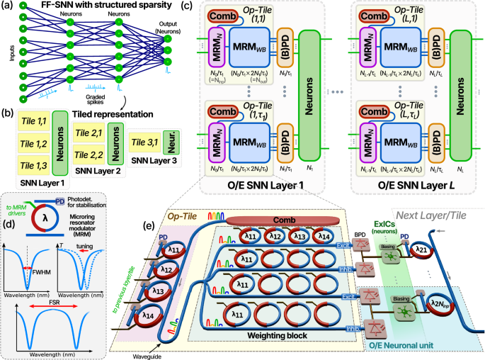
The SEPhIA analog neuromorphic photonic-electronic architecture implements all the required functional blocks for realizing a deep SNN with optical weighting using graded spikes. Due to the lossy nature of realistic photonic components and our design choice of not implementing additional on-chip optical amplifiers within the architecture (primarily due to their footprint), there's an inherent limitation on the photonic circuit size (see further analysis in Discussion). Acknowledging this, we realize a multi-tiled optoelectronic (O/E) SNN which aims to represent SNNs with block-diagonal sparse weighting matrices (see example in Fig. 1a). Sparsely connected deep neural networks offer significantly better suitability for integration in hardware while often incurring minimal use-case dependent decrease in classification accuracy.
These block-diagonal components of a given weighting matrix within an SNN layer can be considered as individual, parallel functional circuits called tiles. The same sparse SNN in the form of tiles is shown in Fig. 1b. In our architecture, these tiles will be referred to as Op-Tiles (optical tiles). Unlike the case of time-domain multiplexed tiled optical processing of matrices, our tiles represent a case of hardware parallelism.
The multi-tiled deep O/E-SNN architecture is shown in Fig. 1c. It consists of neural network layers (total of ), where each -th layer contains one or more (total of ) Op-Tile(s). Each Op-Tile (Fig. 1e) contains (a) a single, multi-wavelength optical source (such as a frequency comb laser), (b) a set of neuronal MRMs, shown in Fig. 1d, followed by (c) MRM-based, WDM-enabled integrated photonic signal routing and weighting circuit (an MRM weight bank, previously experimentally demonstrated as suitable for optical spike weighting). Each Op-Tile has two defining size parameters: number of inputs and number of outputs . is defined by the number of available WDM channels, while is flexible and can be adjusted. In the simplest case where , we can refer to the Op-Tile size . Following the MRM weighting block, the weighted optical signals are summed up on pairwise balanced photodetectors (BPDs) for excitatory and inhibitory functionality, followed by an (optional) transimpedance amplifier (TIA) or other form of amplifier (as a source of gain in the electrical domain). All the outputs from a given l-th layer of parallel Op-Tiles drive a set of analog, electronic excitable integrated CMOS circuits (ExICs, ,where the 1/2 factor accounts for the BPDs), which provide the neuron-like excitable dynamics (=spiking). This set of parallel Op-Tiles and the corresponding electronic neurons constitutes a single layer of the feed-forward SNN.
To validate the idea of our proposed SEPhIA neuromorphic O/E architecture, we provide a comprehensive set of different types of numerical simulations. First, we utilize a Verilog-A based electronic-photonic co-simulation model for time-domain modeling of the O/E neuronal units (consisting of coupled CMOS + MRM), including a compact model of a MOSCAP-based silicon MRM that captures its electrical and optical dynamics. Second, we implement a multi-layer feed-forward O/E-SNN by leveraging the combination of snnTorch framework and our custom PyTorch-based frequency-domain functional simulator of photonic neural networks based on compact photonic device models. Thanks to the use of PyTorch, our O/E-SNN model is end-to-end differentiable and can utilize the autograd engine for true-to-hardware gradient-descent-based O/E-SNN model training.
Device-level co-simulation of the O/E neuronal unit
First, we focus on the O/E neuronal unit as shown in Fig. 1e. There are two main functional parts in an O/E neuronal unit of SEPhIA: a photodetector-coupled analog ExIC, and an MRM. The ExIC implements the nonlinear spiking functionality and generates the action potentials (spikes). We utilize an adaptive exponential leaky integrate-and-fire (AdEx LIF) circuit model (Fig. 2a), with optical inputs enabled via a pair of balanced photodetectors (BPDs) for both excitatory (+) and inhibitory (-) functionality. The AdEx ExICs exhibit spike-frequency adaptation and bursting, where the adaptation current and optional refractory period provide each neuron with an intrinsic, tunable fading memory, the same mechanism that grants adaptive spiking neurons their temporal expressivity. The AdEx LIF circuit also exhibits neural heterogeneity through tunable parameters, enabling the O/E spiking neurons to be configured such that they can produce various types of responses. In this demonstration, a set of individual ExICs is coupled to a set of individual MRMs on a shared bus waveguide (Fig. 2b). A schematic of the coupled photonic-electronic Verilog-A co-simulation model is shown in MRMs (Fig. 2c). In the current architecture, neural outputs are encoded at the MRM through port. Various possible methods of photonic-electronic co-integration are depicted in Fig. 2d.
The transient responses of the four ExICs simulated in Verilog-A when subject to current inputs from Fig. 2e-g are shown in Fig. 2h-j. We demonstrate three different kinds of spiking behaviors at 1GSpike/s rates: in the first regime (Fig. 2e, h, k), the circuit produces a tonic (repeated, regularly spaced) spiking under a constant input with weak adaptation, representing neurons that sustain continuous firing at nearly constant rates, similar to a conventional LIF neuron. In the second case (Fig. 2f, i, l), a spike-frequency adaptation is observed as the neuron is stimulated with a pulsed input current. With each spike, the spike-triggered adaptation mechanism kicks in, increasing the inter-spike interval, and gradually reducing the firing rate as the neuron adapts to the input pulse. Third (Fig. 2g, j, m), we demonstrate bursting dynamics, with a slower adaptation, in which clusters of continuous spikes are followed by quiescent intervals. For each of the regimes of the ExIC, we provide the corresponding time traces (Fig. 2k-m) for the coupled MRM-ExIC system in the neuronal units. These traces show the optical power per wavelength at the output of the shared bus waveguide for the case where the ExIC circuit outputs simultaneously directly modulate the MRMs, with a model case of mW, and demonstrate the viability of ExIC-driven MRMs for WDM spiking photonic architectures.
Figure 3 numerically demonstrates the operation of these MRMs, using a numerically generated comb laser spectrum (in green, see Supplementary Information S2), an ideal transmission spectrum of an MRM (dashed lines) and a pass-through spectrum of multiple MRMs (dark blue). Due to the notch frequency filtering nature of the MRMs, some degree of crosstalk among adjacent modulation channels is inevitable. To evaluate the optimal amount of modulation-induced resonance shifting in the MRM with respect to crosstalk, we aim to maximize a figure of merit (FoM) represented as a sum of the effective extinction ratio (ER) and crosstalk of two adjacent WDM channels, modulated by a single MRM. The figure of merit is shown in a heatmap in Fig. 3e as a function of the ring Q-factor and the on-off keying (OOK) MRM resonance shift , applied to two MRMs operating on adjacent WDM channels. For the depicted case of Q = 7.5K, GHz at 1310 nm, the frequency domain crosstalk-optimized shifting range is observed as pm. This value (and correspondingly scaled values for GHz and GHz) guides the MRM resonance shifting range choices and (for weighting) in the following sections.
Hardware-aware trainable O/E-SNN model
The full O/E-SNN model training procedure flow diagram is shown in Fig. 4a. Thanks to the end-to-end trainable nature of the developed model, the training procedure directly adapts to key aspects of the photonic hardware, such as non-uniform WDM optical channel powers from the multi-wavelength source, the actual optical powers available for each WDM channel, the specific transfer functions of the MRMs, the frequency-domain crosstalk across MRMs, the optical power attenuation at each photonic component and the limited signal-to-noise ratio (SNR). The O/E-SNN is trained using supervised training with backpropagation through time (BPTT) over discrete timesteps using a surrogate arctan function for gradient calculation of LIF spiking neurons during the backward pass.
Figure 4b, c shows an example of O/E-SNN training losses and validation accuracy recorded over 20 epochs for repeated training runs. In this case, we assume all the MRMs' parameters as Q = 10K and ER = 15 dB, and WDM channel spacing of GHz. The full set of simulation parameters is available in the Supplementary Information S2. For the classification problem, we are using a subset (4 classes, similarly to ref. ) of the dimensionally reduced fashion image dataset encoded into rate-coded spike trains (see Supplementary Information S2 for details). Both the curves confirm that the true-to-hardware O/E-SNN model is well trainable, reaching (and exceeding) 90% classification accuracy on the selected problem.
In particular, the O/E-SNN trained in this example is a two-layer O/E-SNN, where the first layer contains two parallel Op-Tiles (as shown in Fig. 1e), each of size (corresponding to a 16 × 16 all-pass MRM weight bank), spiking neurons, and the second layer contains a single Op-Tile with , (corresponding to a 16 × 8 weight bank) followed by spiking neurons. The full tiled O/E-SNN architecture with all the main functional blocks is also shown in the schematic in Fig. 5a.
As an optical source for each Op-Tile, we assume an idealized frequency comb laser source with WDM channels, with uniformly randomly distributed peak optical power within a 2 dB band from the maximum optical power for each comb line. Figure 5b depicts the internal state variables (membrane potentials) of all the LIF neurons (ExICs) in the first layer (for both Op-Tiles in the layer, divided by thick black line in the plot). Figure 5c depicts the corresponding optical spikes at the output of all the O/E neuronal units between first and second O/E-SNN layer. The slight variation in observed output optical powers for different neurons in Fig. 5c comes from the non-uniform optical power distribution of the WDM channels at the multi-wavelength source, and is adapted for, by the physics-aware O/E-SNN training procedure. Figure 5d depicts the membrane potentials at the final layer of neurons, and Fig. 5e depicts the classifier prediction (based on cumulative count of output spikes per each neuron) over all the timesteps. We can observe the cumulative counts reaching a maximum of spikes for neuron 1, corresponding to a correct classification of the input sample. Figure 5f then depicts the confusion matrix for the trained O/E-SNN on the test set, corresponding to total classification accuracy of 91.35% for a sample run with Q = 10K, ER = 16 dB and GHz. We can compare this to two feed-forward SNN baselines of the same size: a fully-connected two-layer (FC-SNN), and a SNN with structured sparsity (Table 1). Using the same training procedure and same dataset, we achieve 93.65% classification accuracy for the FC-SNN benchmark, and 92.97% classification accuracy for the structurally sparse SNN benchmark. This demonstrates that introducing a degree of structured sparsity into the model for the given task yields a classification accuracy that's comparable to a fully-connected model, and also confirms that the performance of our physics-aware O/E-SNN model with noise and crosstalk effects is comparable to that of an ideal SNN, only trailing behind the conventional SNN by percentage point.
Furthermore, the O/E circuit performance is influenced by a complex interplay of various physical characteristics of the system, including MRM parameters (Q-factor, extinction ratio, insertion loss), PD parameters (thermal noise, shot noise and noise equivalent power) and multi-wavelength source characteristics (WDM channel spacing , optical power levels, mode linewidths, noise), among others. The presented model allows us to directly explore the design space of these parameters and their interplay on the selected figure of merit (classifier accuracy) of the O/E-SNN. For WDM channel spacing , we explore three different options: Ⓐ GHz; Ⓑ GHz; and Ⓒ GHz. A corresponding MRM shifting range is set for each . For each , we also explore multiple representative sets of MRM design parameters with various Q-factors and extinction ratios (ER): higher Q MRMs including ① Q = 10K and ER = 15 dB, motivated by realistic MOSCAP MRM device parameters; ② Q = 10K and ER = 6 dB; and lower Q-factor MRMs as ③ Q = 5K and ER = 6 dB. In total, this yields 9 sets of design parameters. In all cases, we assume a fixed set of ideal PD parameters, which yields noise equivalent power (NEP) of or minimum detectable power at 2.5 GHz bandwidth under dark conditions.
We can observe the mean O/E-SNN validation accuracies during training for all the parameter sets in Fig. 6. A total of independent repeated training runs have been performed for each set of parameters. We can see that the lowest overall validation loss was achieved for parameter set Ⓐ ① ( GHz, Q = 10K, ER = 15 dB), that is, for the broadest WDM spacing, and for MRMs with high-Q and high ER. In such case, the frequency domain crosstalk effects have the lowest influence. An overall trend of increase in validation losses can be observed as is decreased, indicating that tighter channel spacing brings crosstalk-related impairments to the system performance. Interestingly, it can be observed that for the lowest tested GHz in Fig. 6c, better performance (lower validation loss) is achieved with ② (ER = 6 dB) rather than ① (ER = 15 dB), indicating that for ultra-dense WDM channel spacing, lower MRM extinction ratio can yield a better performing system, which was not the case for larger WDM channel spacing. This further highlights the complexity of the interplay of various physical effects at the device and circuit level, which must be considered when realizing photonic computing architectures. The minimal observed validation losses are summarized in Table 1.
Additionally, we explore the robustness of the trained O/E-SNN against changes in WDM channel optical power . Figure 7 shows the sweep results for all 9 parameter sets discussed previously. In all the cases, the O/E-SNN was trained with a peak optical power per WDM channel dBm (denoted as a dash-dotted red vertical line in the figure). After the training, a test set classification was performed while sweeping from 12 dBm to -4 dBm, effectively bringing the system outside of operational conditions it was trained for. In the majority of the cases, we observe that highest accuracies are achieved for powers slightly above the selected training , which means the selected represents the lower bound of optical powers under which the system can perform well. In agreement with previous data, we observe the highest degree of robustness for Ⓐ ① ( GHz, Q = 10K, ER = 15 dB). Furthermore, we observe that with decreasing WDM channel spacing, the performance of ② gradually becomes comparable to ①, which is in agreement with the validation loss data in Fig. 6, and we also observe that in the case of Ⓒ ③ (Fig. 7c), the best O/E-SNN performance is effectively capped by the physical effects (cross-talk, noise), further emphasizing that practical challenges can arise for ultra-dense WDM optical computing systems. Interestingly, we also observe slight accuracy drop at optical powers strongly exceeding the value used for training. This can be attributed to the presence of nonlinearity at the photodetectors (where photodetector current ). The maximal observed test accuracies for each parameter set, as well as the accuracy change when is decreased by 3 dB from the optical power corresponding to the maximum accuracy (as a simple robustness measure) are shown in Table 1.
Monte-Carlo functional robustness analysis
Finally, we perform a Monte-Carlo analysis to assess the robustness of the trained O/E-SNN against fabrication-induced photonic component variations and wavelength drift of used optical sources. In all the following cases, we assume a model trained with ideal components (no variation-aware training). First, we focus on variations of the Q-factors and ER in all the MRMs (that is, both neuronal and weighting MRMs across all the Op-Tiles). By assuming that both sidewall roughness of ring waveguides and bus-ring gap follow a normal distribution during fabrication, we obtain approximately log-normal expected distribution of observed loaded Q-factors (see Supplementary Information S5). For the extinction ratio (ER) of microrings outside of critical coupling regime, we assume approximately log-normal distribution, or normal distribution for ER specified in dB. Figure 8a-c shows the mean O/E-SNN accuracies during random sampling of both MRM Q-factors and ERs from their respective distributions, assuming the nominal value represents either the mean (ER in dB) or median (Q) of the distribution while sweeping the standard deviation both from 0% to 30% of the nominal respective value. We observe highest ring variation sensitivity for ③ (Q = 5K, ER = 6 dB), particularly with respect to ER variation, while higher Q-factor cases ① (Q = 10K, ER = 15 dB), ② (Q = 10K, ER = 6 dB) exhibit comparable robustness. Interestingly, some of the highest accuracy degradation across all the three cases is observed in the upper-right heatmap corner - that is, with strong ER variation and little to no variation of MRM Q-factors. This hints at a complex interplay between the MRM parameters at an architecture level, where small but non-zero variations in the ring Q-factor can partially compensate the detrimental effects of large ER variation. Second, we evaluate robustness under wavelength drift during inference across all the WDM channels. We explore two variants: a locked drift (all WDM channels drift by an equal randomly sampled amount, which would be the case in a frequency comb source, Fig. 8d), and a 'non-locked' drift (each WDM channel wavelength drifts independently, such as when using an array of individual lasers, Fig. 8e). We sample the optical wavelength drift randomly from a normal distribution around mean nm with standard deviation ranging from 20 to 80 pm. The mean observed accuracy results indicate comparatively highest robustness against wavelength drift in the Q = 5K case, which can be explained by the lower slope of the low-Q MRM notch filter transfer function. Furthermore, we observe measurably stronger robustness against the wavelength drift in the locked case. This can be explained by the effective weights changing by a proportionally similar amount across the whole network, increasing the likelihood of drift compensation at the balanced PD stage. This further highlights the advantage of using a shared multi-wavelength laser in the O/E-SNN SEPhIA architecture.
Here, we will discuss various scaling related practical constraints and aspects of the proposed architecture, including (i) the area footprint, (ii) the optical power loss link budget limitations, (iii) the frequency domain limitations, (iv) a power consumption analysis (including our choice of MOSCAP MRMs), (v) comparison with existing state-of-the-art in neuromorphic photonics and (vi) suitability of the architecture for processing of temporal datasets.
A first general aspect to consider in terms of an integrated photonic architecture is the area footprint . Arguably the most commonly explored case of spiking photonic laser neurons are multi-section DFB or Fabry-Perot (FP) lasers. In the case of FP lasers, both referenced works report ~1.5 mm cavity length. Since a single device with footprint is used per neuron, the footprint of neural layer with neurons scales . In the case of SEPhIA, the cavity lengths of the used multi-wavelength sources are comparable (0.4 mm to 1.6 mm in ref. , 1.4 mm), but the footprint of neurons within SEPhIA scales only with the number of MRMs with footprint . Given that in silicon photonics, MRM diameters can be <50 μm, and therefore, our shared WDM-laser approach offers significantly reduced footprint and improved scalability prospects. Alternatively, an array of integrated microring lasers could be considered as a footprint-viable optical source option, where the current primary limiting factors are the low maximal achievable levels of output optical power.
In terms of optical power link budget for a single Op-Tile of size (, ), we can consider that a single WDM channel signal from the shared multi-wavelength source must first pass through a series of neural MRMs that encode the spikes, then the signal is optically (spatially) broadcast into waveguides and finally passes through weighting MRMs before detection at the (B)PDs (Fig. 9). Therefore, if we assume a given insertion loss () for all the MRMs in the architecture and if we assume the ideal case of lossless optical power broadcasting (each output of the splitter receives $1/N_"out"$ optical power), we can consider the total minimal power reduction (without spiking or weighting) in dB as . This is plotted in Fig. 9c for for various values of . This estimate represents the power budget solely from the power splitting and losses at each component along the signal pathway and does not represent additional optical power requirements due to channel crosstalk or similar effects.
To get an estimate for optical power per WDM channel, we can take a recent O-band quantum-dot frequency comb laser study, which reported a 2.2 THz bandwidth laser with channel spacing between 25 and 100 GHz, with optical power of 3.5 mW/mode for 50 GHz spacing. Therefore, to remain within the same magnitude of optical powers, we highlight dBm/mode ( mW/mode) in Fig. 9d as an expected upper limit for the optical power source within state-of-the-art without any additional optical amplification. The same optical power value was also previously used in other microring resonator (MRR) based integrated optical computing works. We also assume a requirement of a dynamic range at the PD stage that enables 4 bits of power resolution. For example, if we assume dB (orange line in Fig. 9d), we see that the Op-Tile size is optical power-limited at approximately . This estimation currently does not consider waveguide propagation losses.
In terms of frequency domain limitations, we are constrained by a single free spectral range (FSR) of used MRMs. We can consider a model case of a single SOI MRM with radius and THz at 1310 nm. Using previously reported characteristics of heterogeneous quantum dot (QD) comb lasers, we can consider line spacings 63/31.5/15.5 GHz, and more recently 100/50/25 GHz. Using a simple formula to get the maximum number of resonances within a single MRM FSR range , we obtain numbers ranging from to . While tighter packing of frequency channels towards ultra-dense WDM approaches increases the achievable tile size, they also introduce significant challenges related to channel crosstalk, requirement for high-Q MRMs, and limited power per channel. Limitations related to FSR can also be addressed with the use of interleavers, or through exploiting multiple FSRs. By considering the Op-Tile scaling limitation estimates based on state-of-the-art MRMs and multi-wavelength sources from the perspective of necessary optical power per each WDM channel () and from the perspective of FSR-limit in the frequency domain (the most conservative for the broadest WDM spacing GHz without the use of interleavers or multiple FSRs), we believe the maximum used Op-Tile size selected in our simulations represents a realistic, representative example.
In terms of power consumption, one of the most frequently used figures-of-merit in neuromorphic photonics is the energy per spiking event. At our neuronal unit level, there are power consumption contributions from both the electronic () and optical () domains. To enable accurate estimation of energy consumption in implementations of adaptive LIF neurons, we have developed a power-aware model that explicitly accounts for all major current components contributing to both dynamic and static power dissipation (see Methods). The model also separates dynamic and static power contributions and integrates the total instantaneous power over each spike event to estimate the energy-per-spike, which is directly observable at the model output. Based on transient simulations, the proposed electronic neuron circuit (including 10 fF of ) consumes an average power of approximately μW under typical operating conditions. In terms of optical power, using data from Fig. 7a, we can assume required dBm/channel ( mW/channel in continuous-wave (CW) operation; this is for which full O/E-SNN accuracy is still maintained at 90% before the accuracy roll-off, for the O/E-SNN with GHz and MRM parameters Q = 10K and ER = 15 dB).
The total required power for operating the O/E neuronal unit within the complete O/E-SNN with Op-Tile size is therefore dominated by the optical power contribution, mW. Assuming a case of continuous 1 GSpike/s spike firing rate, this corresponds to 2.516 pJ/spike. Furthermore, we can consider an illustrative case of a minimal spiking interlink (Fig. 9b), where the optical spikes from a single neuronal unit (using one MRM) are being optically weighted by a single non-volatile MRM before reaching the photodetectors. If we therefore consider this minimal architecture with one neural MRM and one weighting MRM (with the same IL = 0.2 dB as in all the other cases) and target the same peak optical power per WDM channel at the PD stage which enabled good performance of the full O/E-SNN, we obtain required dBm, yielding μW and 44 fJ/spike at 1GSpike/s.
While the SEPhIA architecture is in principle not limited to a specific photonic technology, we consider carrier-accumulation MOSCAP MRMs in its implementation. This is motivated by several advantages for both the neuronal and weighting blocks. In an event-driven spiking architecture, the modulator energy should ideally scale with spiking activity rather than with time. MOSCAP MRMs, being capacitive devices with sub-10nA leakage currents (demonstrated on the same material stack) consume energy only during spike transitions, CMRM×Vspike per event, making the E/O conversion energy in the neuronal block directly proportional to network activity. This property aligns naturally with the sparse, event-driven nature of SNN workloads. MOSCAP MRMs have also been shown with sub-volt tuning. Carrier-injection MRMs, in contrast, dissipate continuous current throughout each spike duration to sustain the injected carrier population, and carrier-depletion MRMs, while also capacitive, exhibit lower modulation efficiency in silicon, requiring larger voltage swings and incurring a quadratic energy penalty per spike event. For the weighting block, MOSCAP-based MRMs offer low insertion loss, high modulation efficiency, and absence of thermal crosstalk - all critical requirements for the densely packed Op-Tile architecture in the proposed SEPhIA architecture where multiple MRMs share a single bus waveguide. On the same heterogeneous III-V/Si material stack, insertion losses of ~0.05 dB per device have been measured. Regarding the static power, holding a programmed resonance shift in a MOSCAP requires only its gate leakage current, experimentally measured at the tens-of-picoampere level and corresponding to tuning efficiency of ~5.3 nm/pW (~1 fW/GHz in the O-band) on a related variant of the same platform, at least 9 orders of magnitude below conventional thermal tuning or carrier injection. If we therefore consider an inference-heavy workload with a weight-stationary dataflow (such as the classifier in this work), we can primarily focus on the power consumption from the neuronal modalities. We also want to emphasize that our O/E-SNN processing architecture is fully analog, and therefore ADC-less, thereby avoiding one of the components incurring significant power consumption in optoelectronic computing.
To better position our proposed architecture in the context of existing state-of-the-art, we have selected a set of representative published works focusing on optoelectronic and all-optical devices and circuits within the context of SNNs. Table 2 summarizes the comparison in terms of neuron design, possible or proposed network architecture by the reference, neuron dynamics type, maximum firing rate of the neuron, energy per spike, and scalability score of the implementation. Each implementation is graded according to five categories for scalability score: footprint, packaging, WDM, maturity of the fabrication, and cascadability without additional resources (see Supplementary Information S3 for more details on the scoring). Additional details on the calculation of the output optical energy per spiking period are included in the Supplementary Information S4. Beyond the photonic spiking neuron implementations included in Table 2, it is also worth mentioning photonic nonlinear (neuronal) devices that are not spiking, yet exhibit a short-term internal memory effect that is similar to LIF neurons.
In terms of all-optical spiking nodes, spiking can be achieved through various means, either by relying on nonlinear dynamical responses in lasers via injection locking, the interaction between a slow thermal nonlinearity and fast free carrier effects in microring resonators, or by using multi-section laser devices. All-optical spiking devices offer the generally highest spiking operation speeds, with the highest firing rates reported from membrane III-V/Si integrated lasers exceeding 12.5 GSpike/s. However, scalability typically represents a challenge. On-chip lasers, as active photonic devices, suffer from complex integration challenges and are often bulky components (up to mm2/device footprint for Fabry-Perot designs). Injection locking of lasers requires precise control of the input optical signal (wavelength, power, polarization), which hinders scalability, and presents limitations with respect to fan-in from other coherent photonic neurons. Wavelength control (for WDM) realized with multiple individual lasers adds a further degree of complexity. Similarly, the free-space photonic links require bulky setups. Multiport interferometer network architectures are typically aimed at coherent operation and are less suitable for WDM. At the time of this manuscript's writing, graphene, phase change materials (PCM), and memristive junctions do not rely on mature fabrication platforms. Lastly, even though multiple references reported their neurons' cascadability, the fan-out of a single neuron's output is only reasonable at moderate levels, ~10-15 post-synaptic neurons, due to limited output spike ER, the coupling and propagation losses, excitability threshold of the neurons, etc. Therefore, these architectures require an amplification stage in between the SNN layers. We conclude that only the optoelectronic neurons with closely integrated MRMs are marked in the 'cascadable without amplifier' category. We also calculate the approximate optical output energy of the neurons over a single spike period (), to further emphasize the challenges in cascading of neuronal responses in some neurons due to the energy difference between spike activation and spike output energy. As a final remark, all-optical spiking methods typically do not offer neural heterogeneity, as well as other modalities such as layer-wide neural inhibition, winner-take-all firing or practical monitoring of internal neural state variables (like membrane potentials, corresponding to carrier dynamics in lasers), all of which might prove beneficial for SNN operation and experimental training procedures.
Finally, while the proof-of-concept simulation for SEPhIA is benchmarked on a rate-encoded subset of the standard image classification dataset, we want to emphasize that SEPhIA is not architecturally restricted to static data, as it is a temporal processor by design. As described in Results, the O/E-SNN operates on spike trains with a rate-coded representation drawn for every sample, while the model is trained end-to-end with BPTT and the classification is then decoded from the cumulative spike count over time. Hence, the temporal credit-assignment methodology required for sequence processing is already in place. Since the O/E front-end with neural MRMs and BPDs is spike-driven, natively event-based signals can be input directly, requiring changes only to the input-encoding stage. For example, address-events from a neuromorphic/DVS vision sensor can map directly onto WDM channels, analogous to established event-vision SNN benchmarks such as N-MNIST, DVS-Gesture, and CIFAR10-DVS. A second example is intensity-modulation/direct-detection in short-reach optical links, where the received signal is inherently temporal, and recovering the transmitted data to the accuracy required by communication standards is a task that compact SNNs can solve. SEPhIA is a natural fit here, since it works directly in the telecom O-band (1310 nm), allowing for direct processing of optical input signals.
In summary, we have introduced SEPhIA - an integrated optoelectronic WDM-enabled SNN hardware architecture that combines excitable analog CMOS circuits with compact, integrated photonic devices (MRMs) and multi-wavelength lasers shared per multiple neurons. By considering scalability as a key enabling principle, we have devised the optical tile (Op-Tile) as a functional building block of our O/E-SNN, and evaluated the scaling of these tiles from the perspectives of both realistic optical power budgets and frequency domain limitations. Using the estimated realistic optical tile size (), we have hardware-software co-designed the SEPhIA architecture as a multi-tiled, structurally sparse, feed-forward, all-MRM-based WDM-enabled O/E-SNN architecture. We have validated this architecture both at the device (neuron) level, as well as a two-layer SNN classifier using physics-aware BPTT training. We have demonstrated the operation of the O/E-SNN classifier using a widely-used academic benchmarking task (four-class image classification) with rate-based encoding of feature values. Furthermore, we have demonstrated how photonic device parameters and device variance influence the performance (a classification accuracy) at a full SNN level. Finally, we have provided a comparison with other spiking neuromorphic approaches, demonstrating favorable energy/spike metrics. We believe that our O/E-SNN architecture provides a solution to neuromorphic photonic computing that is practically feasible and realistically scalable while offering high computational expressivity for solving non-trivial (temporal) tasks. For future work, we envision a broad set of characteristics that can be further incorporated and explored in the simulations, including quantization (limited bit precision) of photonic modulator states, additional noise sources and different analog neural circuits, among others; as well as more advanced methods for introducing layer sparsity or use of datasets that are natively temporal, spike-based or in the optical domain, such as various time-series data, sensor data or telecommunication data streams.
Verilog-A model of the O/E neuronal unit
To facilitate co-simulation of the MRM with electronic components, we have implemented compact Verilog-A models. While numerous approaches have been explored for integrating photonic devices such as MRMs and photodetectors with electronic integrated circuit design, embedding photonic models directly in SPICE (which is widely used for circuit design) offers a more efficient workflow, saving significant time and effort during the design phase.
The AdEx LIF model (Fig. 2a) was implemented in TSMC 28 nm process and is modeled as a set of coupled differential equations. The membrane potential, , dynamics are governed by a balance between capacitive charging through the membrane capacitance, , leakage currents controlled by the leakage conductance, along with the resting potential, , an adaptation current, and externally applied input current, . The spike is initiated first through an exponential term parameterized by the threshold potential and the slope factor, .
Adaptation is introduced through the current which evolves with a time constant . Parameter controls the strength of the subthreshold depolarization that drives the adaptation, while determines the discrete increment of adaptation that occurs after each spike.
The membrane potential, , is reset to its reset potential , when it crosses its threshold voltage while the spike-triggered adaptation is governed by . As the adaptation grows, it provides negative feedback to the membrane potential, shaping the temporal structure of spiking activity. The interaction between these elements produces a diverse set of spiking behaviors (Fig. 2).
The neuronal model is further coupled to the MOSCAP MRM circuit. The electrical subcircuit of the MOSCAP MRM represents the gated waveguide section as a bias-dependent MOS capacitance, , derived from accumulation-depletion-inversion behavior, in parallel with any additional parasitic capacitance. This capacitive load is driven through a series access resistance, . A dedicated internal node, , is introduced between the ExIC and the MOSCAP to account for the RC-limited charging behavior, ensuring that the voltage used for refractive index and absorption change calculations reflects the actual gate dynamics rather than the ideal drive waveform. As the MOSCAP MRM's RC time constant and carrier dynamics both operate well beneath the ~1 ns spike period, the temporal response of the O/E neuronal unit is limited by the analog CMOS ExIC rather than the photonic modulator, offering a favorable scaling path toward higher spiking rates at more advanced CMOS nodes. The bias-dependent capacitance , effective index change , and absorption change are obtained from polynomial fits to measured or simulated device data, and carrier-density data using plasma dispersion and free-carrier absorption relations. The optical submodel employs time-domain coupled-mode theory to describe the evolution of the intracavity field amplitudes with resonance detuning determined by and round-trip loss modified by . This framework enables accurate prediction of the modulators' through- and drop-port optical powers under arbitrary electrical drive signals, while preserving physical parameters such as ring radius, coupling coefficient, and quality factor of microrings.
For the power consumption analysis, the membrane capacitance current models the charging/discharging of the membrane node and dominates the dynamic power during spike initiation and repolarization, calculated as, . The leakage current models the steady-state conductance pulling the membrane potential toward its resting potential, given by , and contributes to static power even in the absence of spiking activity. The exponential spike current captures the activation of channel dynamics near threshold, defined as and dominates the dynamic power during spike onset. To reflect adaptation dynamics, the model also includes an adaptation capacitance that captures the transient charging/discharging during spikes, , where is the adaptation-state potential. This current modeling the continuous adaptation dynamics contributes an additional component to the dynamic power at spike events. In addition, the model includes the buffer-driving current for the microring's MOSCAP load, , which accounts for the extra energy required to drive the spike output into the optical modulator interface. All these currents are explicitly sourced from the supply rail to ensure realistic power accounting during SPICE-level simulations.
Furthermore, our model considers closed-loop feedback with an additional PD at the drop port of the MRMs (see Fig. 2b). In WDM systems, where adjacent channel resonances can lead to significant crosstalk, such closed-loop bias stabilization is essential. Our work extends prior demonstrations of automatic wavelength stabilization via bias control of MRMs, which dynamically adjusts the ring bias to align and hold the resonance wavelength per channel under varying operating conditions. The high-speed electrical bias tuning in our design enables each ring to be locked to its optimal wavelength with minimal latency, ensuring stable, low-crosstalk performance across all channels. By actively stabilizing the microring resonance through electrical bias modulation and monitoring, our approach avoids the slower response of purely thermal tuning methods while maintaining robust wavelength alignment across all channels.
Compact MRM model in the O/E-SNN
For all the MRMs in the O/E-SNN models (that is, both the neuronal MRMs and weighting MRMs), we represent each individual MRM using its input-output transmission (attenuation) characteristic. This compact device model assumes the all-pass MRM through-port transmission as an ideal, Lorentzian-based notch filter. Assuming is the resonance frequency of the MRM and is the Q-factor of the MRM, the notch filter spectral full-width at half-maximum (FWHM) is denoted as .
The attenuation of the MRM at a through port (denoted as ) is modeled as:
where is the investigated optical frequency (corresponding for example to a given input WDM channel frequency), is the relative through power at the maximum extinction ratio (ER), is the relative pass-through power accounting for device insertion loss (IL) and is the spectral half-width at half-maximum (HWHM). Since the system is operated in a WDM, non-coherent regime, phase-shifts at a component level are not considered in the current numerical model. We also currently do not consider the additional passbands (outside of the main resonant frequency) introduced by the MRM's finite free spectral range (FSR) during individual device modeling. Instead, we ensure that an individual Op-Tile operates within a single FSR range of used MRMs (see frequency domain limitations in the Discussion). We assume that all the all-pass MRMs in the whole architecture (that is, both in the neural layer as well as in the weighting layer) have equivalent properties, namely their Q-factor, ER, and IL, and also assume a fixed notch filter shape (that is, fixed Q-factor and ER) during the MRM tuning. In the presented results, we assume continuously tunable MRM resonances of the MRMs in the weight bank, that is, without resonance tuning (modulation) quantization. We currently model the SEPhIA architecture with all-pass MRMs, but add-drop MRMs can also be utilized to reduce the weight bank ring count in half (while introducing reduced ER for inhibition at the MRM drop port).
Training of the O/E-SNN model
As highlighted in Fig. 1, the current SEPhIA architecture utilizes a standard MRM weight bank design with all-pass MRMs. The odd rows of the MRM weight bank realize excitatory synaptic functionality, while the even rows realize inhibitory synaptic functionality. The trainable parameters of the model directly correspond to the individual resonance wavelength detuning of each all-pass r-th row, c-th column MRM in -th Op-Tile of -th layer. To effectively limit the MRM resonance shifting range, the model utilizes sigmoid-based clamping of the trainable weights to the desired MRM resonance wavelength shifting interval denoted as . In all cases, positive weight assumes a negative MRM resonance wavelength shift (resonance blue-shift). For both weighting and neuronal MRMs, we assume an ideal case of low, fixed insertion loss (IL) of 0.2 dB following state-of-the-art for silicon MRMs.
In addition to MRMs, a second set of trainable parameters models a programmable electrical gain within each neuronal unit, and is intended to provide an (optional) trainable degree of freedom in the model for compensation of lack of optical gain blocks in the signal pathway. The ExIC functionality is modeled using a block of Leaky Integrate and Fire (LIF, snnTorch.Leaky()) neurons, which were extended to optionally exhibit an absolute refractory period to implement some aspects of the adaptive model. The refractory period can be optionally specified in the number of timesteps.
We train the O/E-SNN using an AdamW optimizer with cosine learning rate scheduling (targeting lr = 0 at the end of the final epoch). We use the optimizer without weight decay, as we have observed better achieved accuracies without the additional L2 regularization term. We use cross-entropy loss (CELoss) with decoding based on max-over-time-membrane potential (MOTM), where the membrane potential of the desired class is encouraged to increase (and vice versa for the non-desired classes). By extension, this maximizes the number of spikes over the simulation run time at the neuron corresponding to the desired class. Alternative coding approaches include end-over-time-membrane (EOTM) or time-to-first-spike (TTFS), among others. Prior to the neuronal units, we utilize conventional Dropout blocks (p = 0.15) to increase robustness of the neural network training. The explored O/E-SNN has a total of 660 trainable parameters, with 640 parameters corresponding to positive-valued resonance shifts of the programmable MRMs in the weight banks (320 for excitatory and 320 for inhibitory connections).
The limited signal-to-noise ratio present in the model is primarily implemented at the photodetector level. The balanced photodetector is modeled as a pair of simplified PDs converting the light signals, represented as complex electromagnetic field , to current , where corresponds to the photodetector responsivity. Furthermore, the PDs incorporate two noise effects: the thermal (Nyquist-Johnson) noise with variance and the shot noise with variance. The simultaneous effect of the two noise effects is modeled at every timestep as a Gaussian white noise with variance described as a sum of the individual effect variances. All used parameter values can be found in the Supplementary Information. Our simulator currently does not model any thermal crosstalk effects among photonic devices.