Intel Partners with Tesla and SpaceX on Terafab | NextBigFuture.com
Intel is now officially partnering with Tesla, SpaceX, and xAI on the Terafab project.
Terafab is their joint venture for a massive, vertically integrated semiconductor facility (primarily in Austin, Texas) that combines logic chips, memory (HBM), advanced packaging, testing, and even photomask production all under one roof. The goal is to produce ~1 TW/year of AI compute capacity -- enough to power billions of Optimus robots, FSD/robotaxi systems, Grok-level training, and space-hardened chips (e.g., D3 for orbital AI) -- far beyond what current foundries like TSMC or Samsung can supply at the needed scale and speed
Intel's Role is to Help Remake Silicon Fab Technologyr
Intel's stated contribution is to help refactor silicon fab technology by bringing its expertise in chip design, fabrication, and packaging at ultra-high scale. This directly supports Terafab's production targets and modernization of the overall process.
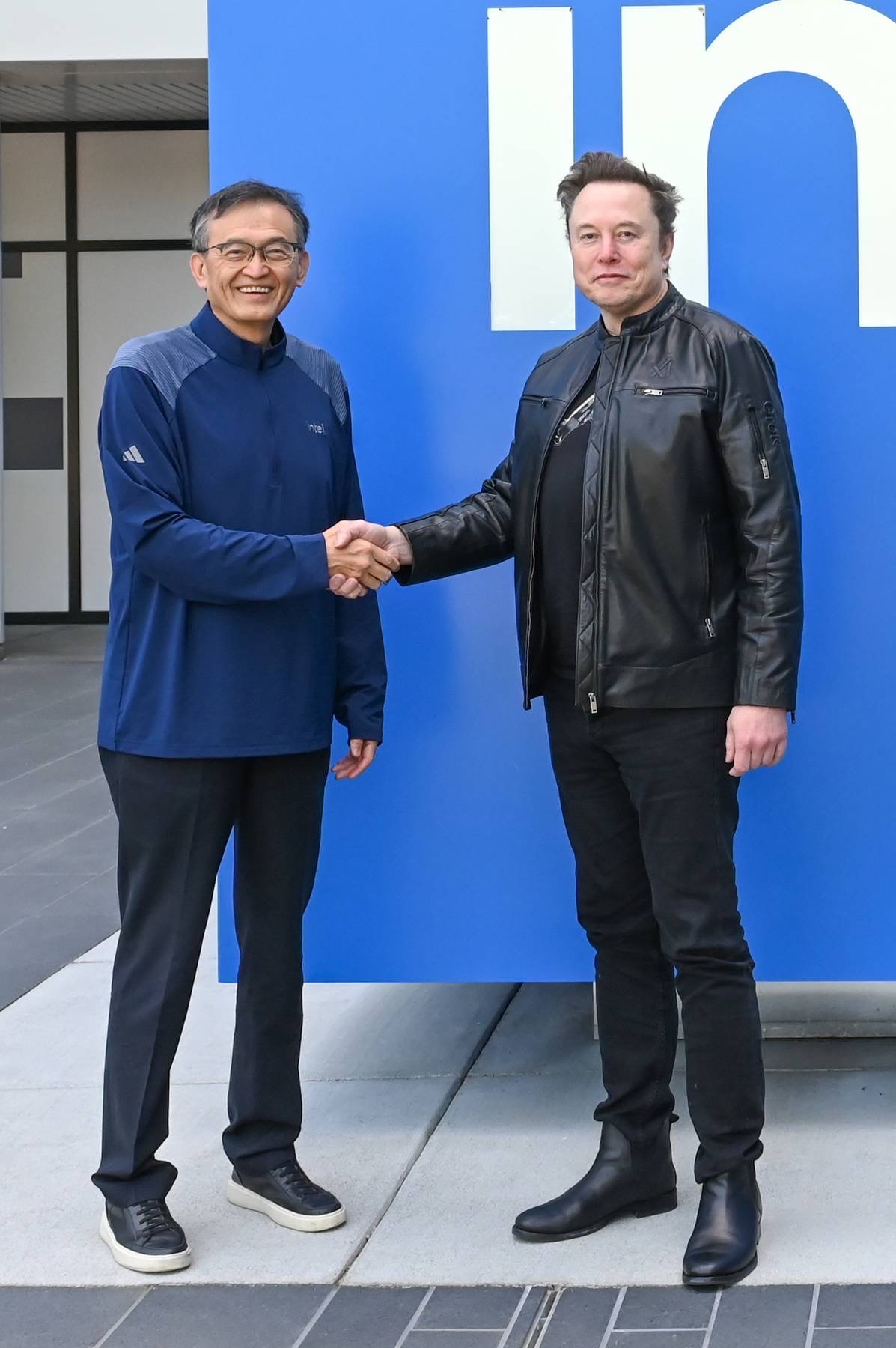
Intel hosted Elon Musk at its facilities last weekend, signaling active, high-level engagement (a handshake photo from the meeting was shared in related posts).
Tesla/xAI/SpaceX already design their own AI silicon (AI5/AI6 for terrestrial use, D3 for space). They will combine that with Intel's manufacturing strengths for much faster feedback loops than a traditional foundry relationship would allow.
Intel's foundry business (Intel Foundry / formerly IFS) is in the middle of a multi-year turnaround that accelerated sharply in 2025-2026 under CEO Lip-Bu Tan. The strategy shifted to a disciplined Foundry First focus. They are prioritizing high-margin external customers, yield execution, and capital discipline while still serving Intel's internal needs.
Key Technical & Operational Progress
Intel 18A (1.8 nm-class) node entered high-volume manufacturing (HVM) in late 2025 / early 2026, completing the "5 Nodes in 4 Years" roadmap. It's Intel's first node with RibbonFET (gate-all-around) transistors + PowerVia (backside power delivery). Yields are reported in the 60-75% range (improving toward 80%+ by 2027 for full profitability). This is already powering Intel's own Panther Lake and Clearwater Forest chips, with external customer silicon ramping.
Advanced packaging (EMIB, Foveros, etc.) is a bright spot and a major revenue driver. Intel is positioning itself as a strong alternative/backup to TSMC for chiplet-based AI designs.
Next node 14A (1.4 nm-class) is in early customer engagement. Intel has said it will only add significant capacity with firm external commitments -- a clear break from past overbuilding.
Government Backing (Major De-Risking)
CHIPS Act: $7.86 billion direct grant + up to $11 billion in loans for U.S. fab expansion (Arizona, Ohio, New Mexico, Oregon). Additional $3 billion for a Secure Enclave program.
Equity investment: U.S. government took 9.9% stake ($8.9 billion) in 2025, further aligning national-security interests with Intel's success